The Diode

  • As mentioned, a diode is made from a small piece of semiconductor material, usually, silicon, in which half is doped as a p region and half is doped as an n region with a pn junction and depletion region in between;
  • The p region is called the anode and is connected to a conductive terminal;
  • The n region is called the cathode and is connected to a second conductive terminal;
  • The basic diode structure and schematic symbol are shown in Figure 2–1;

figure-2-1

Typical Diode Packages

  • Several common physical configurations of through-hole
    mounted diodes are illustrated in Figure 2–2(a);

figure-2-2

  • The anode (A) and cathode (K) are indicated on a diode in several ways, depending on the type of package;
  • The cathode is usually marked by a band, a tab, or some other feature;
  • On those packages where one lead is connected to the case, the case is the cathode;


Surface-Mount Diode Packages

  • Figure 2–2(b) shows typical diode packages for surface mounting on a printed circuit board;
  • The SOD and SOT packages have gull-wing shaped leads;
  • The SMA package has L-shaped leads that bend under the package;
  • The SOD and SMA types have a band on one end to indicate the cathode;
  • The SOT type is a three-terminal package in which there are either one or two diodes;
  • In a single-diode SOT package, pin 1 is usually the anode and pin 3 is the cathode;
  • In a dual-diode SOT package, pin 3 is the common terminal and can be either the anode or the cathode;
  • Always check the datasheet for the particular diode to verify the pin configurations;


Diode Operation

  • A diode is a two-terminal semiconductor device formed by two doped regions of silicon separated by a pn junction;
  • In this chapter, the most common category of diode, known as the general-purpose diode, is covered;
  • Other names, such as rectifier diode or signal diode, depend on the particular type of application for which the diode was designed;
  • You will learn how to use a voltage to cause the diode to conduct current in one direction and block it in the other direction;
  • This process is called biasing;


PROBLEMS

Answers to all odd-numbered problems are at the end of the book

BASIC PROBLEMS

Section 1–1

The Atom
1. If the atomic number of a neutral atom is 6, how many electrons does the atom have? How many protons?
2. What is the maximum number of electrons that can exist in the 3rd shell of an atom?

Section 1–2

Materials Used in Electronics
3. For each of the energy diagrams in Figure 1–21, determine the class of material based on
relative comparisons.
4. A certain atom has four valence electrons. What type of atom is it?
5. In a silicon crystal, how many covalent bonds does a single atom form?

figure-1-21

Section 1–3

Current in Semiconductors
6. What happens when heat is added to silicon?
7. Name the two energy bands at which current is produced in silicon.

Section 1–4

N-Type and P-Type Semiconductors
8. Describe the process of doping and explain how it alters the atomic structure of silicon.
9. What is antimony? What is boron?

Section 1–5

The PN Junction
10. How is the electric field across the pn junction created?
11. Because of its barrier potential, can a diode be used as a voltage source? Explain.

SELF-TEST

Answers can be found at www.pearsonhighered.com/floyd

Section 1–1

1. Every known element has
(a) the same type of atoms (b) the same number of atoms
(c) a unique type of atom (d) several different types of atoms
2. An atom consists of
(a) one nucleus and only one electron (b) one nucleus and one or more electrons
(c) protons, electrons, and neutrons (d) answers (b) and (c)
3. The nucleus of an atom is made up of
(a) protons and neutrons (b) electrons
(c) electrons and protons (d) electrons and neutrons
4. Valence electrons are
(a) in the closest orbit to the nucleus (b) in the most distant orbit from the nucleus
(c) in various orbits around the nucleus (d) not associated with a particular atom
5. A positive ion is formed when
(a) a valence electron breaks away from the atom
(b) there are more holes than electrons in the outer orbit
(c) two atoms bond together
(d) an atom gains an extra valence electron

Section 1–2

6. The most widely used semiconductive material in electronic devices is
(a) germanium (b) carbon (c) copper (d) silicon
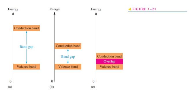
7. The difference between an insulator and a semiconductor is
(a) a wider energy gap between the valence band and the conduction band
(b) the number of free electrons
(c) the atomic structure
(d) answers (a), (b), and (c)
8. The energy band in which free electrons exist is the
(a) first band (b) second band (c) conduction band (d) valence band

9. In a semiconductor crystal, the atoms are held together by
(a) the interaction of valence electrons (b) forces of attraction
(c) covalent bonds (d) answers (a), (b), and (c)
10. The atomic number of silicon is
(a) 8 (b) 2 (c) 4 (d) 14
11. The atomic number of germanium is
(a) 8 (b) 2 (c) 4 (d) 32
12. The valence shell in a silicon atom has the number designation of
(a) 0 (b) 1 (c) 2 (d) 3
13. Each atom in a silicon crystal has
(a) four valence electrons
(b) four conduction electrons
(c) eight valence electrons, four of its own and four shared
(d) no valence electrons because all are shared with other atoms

Section 1–3

14. Electron-hole pairs are produced by
(a) recombination (b) thermal energy (c) ionization (d) doping
15. Recombination is when
(a) an electron falls into a hole
(b) a positive and a negative ion bond together
(c) a valence electron becomes a conduction electron
(d) a crystal is formed
16. The current in a semiconductor is produced by
(a) electrons only (b) holes only (c) negative ions (d) both electrons and holes

Section 1–4

17. In an intrinsic semiconductor,
(a) there are no free electrons
(b) the free electrons are thermally produced
(c) there are only holes
(d) there are as many electrons as there are holes
(e) answers (b) and (d)
18. The process of adding an impurity to an intrinsic semiconductor is called
(a) doping (b) recombination (c) atomic modification (d) ionization
19. A trivalent impurity is added to silicon to create
(a) germanium (b) a p-type semiconductor
(c) an n-type semiconductor (d) a depletion region
20. The purpose of a pentavalent impurity is to
(a) reduce the conductivity of silicon (b) increase the number of holes
(c) increase the number of free electrons (d) create minority carriers
21. The majority carriers in an n-type semiconductor are
(a) holes (b) valence electrons (c) conduction electrons (d) protons
22. Holes in an n-type semiconductor are
(a) minority carriers that are thermally produced
(b) minority carriers that are produced by doping
(c) majority carriers that are thermally produced
(d) majority carriers that are produced by doping

Section 1–5

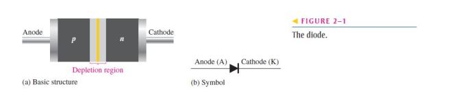
23. A pn junction is formed by
(a) the recombination of electrons and holes
(b) ionization
(c) the boundary of a p-type and an n-type material
(d) the collision of a proton and a neutron
24. The depletion region is created by
(a) ionization (b) diffusion (c) recombination (d) answers (a), (b), and (c)
25. The depletion region consists of
(a) nothing but minority carriers (b) positive and negative ions
(c) no majority carriers (d) answers (b) and (c)


TRUE/FALSE QUIZ

Answers can be found at www.pearsonhighered.com/floyd

1. An atom is the smallest particle in an element.
2. An electron is a negatively charged particle.
3. An atom is made up of electrons, protons, and neutrons.
4. Electrons are part of the nucleus of an atom.
5. Valence electrons exist in the outer shell of an atom.
6. Crystals are formed by the bonding of atoms.
7. Silicon is a conductive material.
8. Silicon doped with p and n impurities has one pn junction.
9. The p and n regions are formed by a process called ionisation.

Key Terms

Atom – The smallest particle of an element that possesses the unique characteristics of that element.
Barrier potential – The amount of energy required to produce full conduction across the pn junction in forward bias.
Conductor – A material that easily conducts electrical current.
Crystal – A solid material in which the atoms are arranged in a symmetrical pattern.
Doping – The process of imparting impurities to an intrinsic semiconductive material in order to control its conduction characteristics.
Electron – The basic particle of negative electrical charge.
Free electron – An electron that has acquired enough energy to break away from the valence band of the parent atom; also called a conduction electron.
Hole – The absence of an electron in the valence band of an atom.
Insulator – A material that does not normally conduct current.
Ionisation – The removal or addition of an electron from or to a neutral atom so that the resulting atom (called an ion) has a net positive or negative charge.
Orbital – Subshell in the quantum model of an atom.
PN junction – The boundary between two different types of semiconductive materials.
Proton –  The basic particle of positive charge.
Semiconductor – A material that lies between conductors and insulators in its conductive properties. Silicon, germanium, and carbon are examples.
Shell – An energy band in which electrons orbit the nucleus of an atom.
Silicon – A semiconductive material.
Valence – Related to the outer shell of an atom.


Section 1–5

  • A pn junction is formed when part of a material is doped n-type and part of it is doped p-type. A depletion region forms starting at the junction that is devoid of any majority carriers. The depletion region is formed by ionisation;
  • The barrier potential is typically 0.7 V for a silicon diode and 0.3 V for germanium;


Section 1–4

  • An n-type semiconductive material is created by adding impurity atoms that have five valence electrons. These impurities are pentavalent atoms. A p-type semiconductor is created by adding impurity atoms with only three valence electrons. These impurities are trivalent atoms;
  • The process of adding pentavalent or trivalent impurities to a semiconductor is called  doping;
  • The majority carriers in an n-type semiconductor are free electrons acquired by the doping process, and the minority carriers are holes produced by thermally generated electron-hole pairs. The majority carriers in a p-type semiconductor are holes acquired by the doping process, and the minority carriers are free electrons produced by thermally generated electron-hole pairs;


Section 1–3

  • The valence electrons that manage to escape from their parent atom are called conduction electrons or free electrons. They have more energy than the electrons in the valence band and are free to drift throughout the material;
  • When an electron breaks away to become free, it leaves a hole in the valence band creating what is called an electron-hole pair. These electron-hole pairs are thermally produced because the electron has acquired enough energy from external heat to break away from its atom;
  • A free electron will eventually lose energy and fall back into a hole. This is called recombination. Electron-hole pairs are continuously being thermally generated so there are always free electrons in the material;
  • When a voltage is applied across the semiconductor, the thermally produced free electrons move toward the positive end and form the current. This is one type of current and is called electron current;
  • Another type of current is the hole current. This occurs as valence electrons move from hole to hole creating, in effect, a movement of holes in the opposite direction;