- To increase the number of holes in intrinsic silicon, trivalent impurity atoms are added;
- These are atoms with three valence electrons such as boron (B), indium (In), and gallium (Ga);
- As illustrated in Figure 1–18, each trivalent atom (boron, in this case) forms covalent bonds with four adjacent silicon atoms;
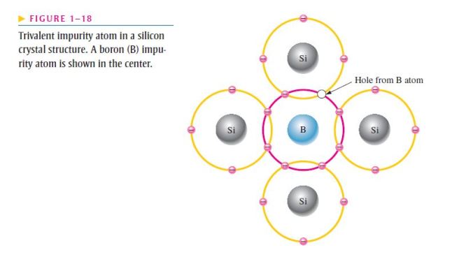
- All three of the boron atom’s valence electrons are used in the covalent bonds;
- Since four electrons are required, a hole results when each trivalent atom is added;
- Because the trivalent atom can take an electron, it is often referred to as an acceptor atom;
- The number of holes can be carefully controlled by the number of trivalent impurity atoms added to the silicon;
- A hole created by this doping process is not accompanied by a conduction (free) electron;
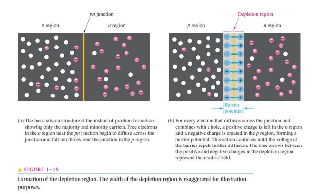
Majority and Minority Carriers
- Since most of the current carriers are holes, silicon (or germanium) doped with trivalent atoms is called a p-type semiconductor;
- The holes are the majority carriers in p-type material;
- Although the majority of current carriers in p-type material are holes, there are also a few conduction-band electrons that are created when electron-hole pairs are thermally generated;
- These conduction-band electrons are not produced by the addition of the trivalent impurity atoms;
- Conduction-band electrons in p-type material are the minority carriers;