- When you take a block of silicon and dope part of it with a trivalent impurity and the other part with a pentavalent impurity, a boundary called the pn junction is formed between the resulting p-type and n-type portions;
- The pn junction is the basis for diodes, certain transistors, solar cells, and other devices, as you will learn later;
- A p-type material consists of silicon atoms and trivalent impurity atoms such as boron;
- The boron atom adds a hole when it bonds with the silicon atoms;
- However, since the number of protons and the number of electrons are equal throughout the material, there is no net charge in the material and so it is neutral;
- An n-type silicon material consists of silicon atoms and pentavalent impurity atoms such as antimony;
- As you have seen, an impurity atom releases an electron when it bonds with four silicon atoms;
- Since there is still an equal number of protons and electrons (including the free electrons) throughout the material, there is no net charge in the material and so it is neutral;
- If a piece of intrinsic silicon is doped so that part is n-type and the other part is p-type, a pn junction forms at the boundary between the two regions and a diode is created, as indicated in Figure 1–19(a);
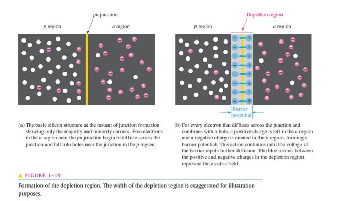
- The p region has many holes (majority carriers) from the impurity atoms and only a few thermally generated free electrons (minority carriers);
- The n region has many free electrons (majority carriers) from the impurity atoms and only a few thermally generated holes (minority carriers);
