- The free electrons in the n region are randomly drifting in all directions;
- At the instant of the pn junction formation, the free electrons near the junction in the n region begin to diffuse across the junction into the p region where they combine with holes near the junction, as shown in Figure 1–19(b);
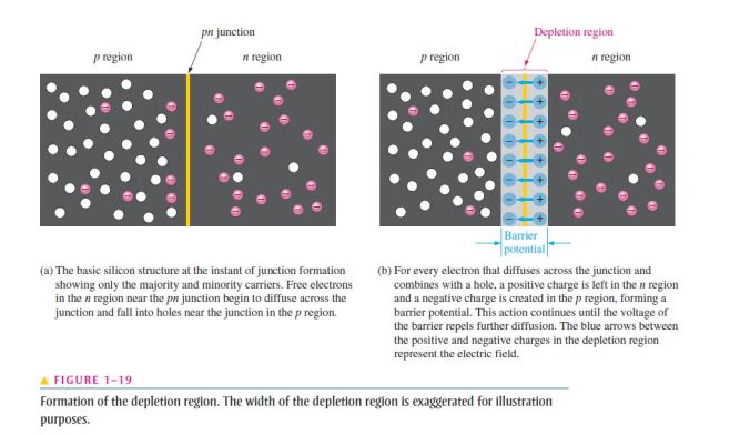
- Before the pn junction is formed, recall that there are as many electrons as protons in the n-type material, making the material neutral in terms of net charge;
- The same is true for the p-type material;
- When the pn junction is formed, the n region loses free electrons as they diffuse across the junction;
- This creates a layer of positive charges (pentavalent ions) near the junction;
- As the electrons move across the junction, the p region loses holes as the electrons and holes combine;
- This creates a layer of negative charges (trivalent ions) near the junction;
- These two layers of positive and negative charges form the depletion region, as shown in Figure 1–19(b);
- The term depletion refers to the fact that the region near the pn junction is depleted of charge carriers (electrons and holes) due to diffusion across the junction;
- Keep in mind that the depletion region is formed very quickly and is very thin compared to the n region and p region;
- After the initial surge of free electrons across the pn junction, the depletion region has expanded to a point where equilibrium is established and there is no further diffusion of electrons across the junction;
- This occurs as follows;
- As electrons continue to diffuse across the junction, more and more positive and negative charges are created near the junction as the depletion region is formed;
- A point is reached where the total negative charge in the depletion region repels any further diffusion of electrons (negatively charged particles) into the p region (like charges repel) and the diffusion stops;
- In other words, the depletion region acts as a barrier to the further movement of electrons across the junction;
Barrier Potential
- Any time there is a positive charge and a negative charge near each other, there is a force acting on the charges as described by Coulomb’s law;
- In the depletion region there are many positive charges and many negative charges on opposite sides of the pn junction;
- The forces between the opposite charges form an electric field, as illustrated in Figure 1–19(b) by the blue arrows between the positive charges and the negative charges;
- This electric field is a barrier to the free electrons in the n region, and energy must be expended to move an electron through the electric field;
- That is, external energy must be applied to get the electrons to move across the barrier of the electric field in the depletion region;
- The potential difference of the electric field across the depletion region is the amount of voltage required to move electrons through the electric field;
- This potential difference is called the barrier potential and is expressed in volts;
- Stated another way, a certain amount of voltage equal to the barrier potential and with the proper polarity must be applied across a pn junction before electrons will begin to flow across the junction;
- You will learn more about this when we discuss biasing in Chapter 2;
- The barrier potential of a pn junction depends on several factors, including the type of semiconductive material, the amount of doping, and the temperature;
- The typical barrier potential is approximately 0.7 V for silicon and 0.3 V for germanium at 25°C;
- Because germanium devices are not widely used, silicon will be used throughout the rest of the book;
