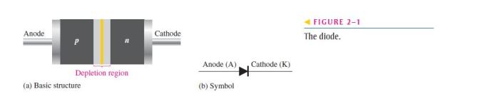
- As mentioned, a diode is made from a small piece of semiconductor material, usually, silicon, in which half is doped as a p region and half is doped as an n region with a pn junction and depletion region in between;
- The p region is called the anode and is connected to a conductive terminal;
- The n region is called the cathode and is connected to a second conductive terminal;
- The basic diode structure and schematic symbol are shown in Figure 2–1;
Typical Diode Packages
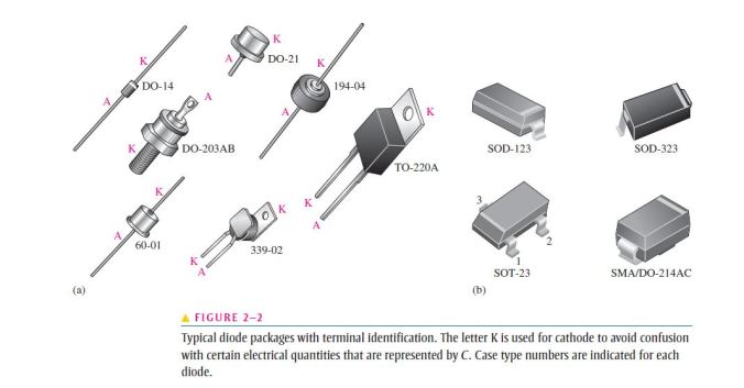
- Several common physical configurations of through-hole
mounted diodes are illustrated in Figure 2–2(a);
- The anode (A) and cathode (K) are indicated on a diode in several ways, depending on the type of package;
- The cathode is usually marked by a band, a tab, or some other feature;
- On those packages where one lead is connected to the case, the case is the cathode;
Surface-Mount Diode Packages
- Figure 2–2(b) shows typical diode packages for surface mounting on a printed circuit board;
- The SOD and SOT packages have gull-wing shaped leads;
- The SMA package has L-shaped leads that bend under the package;
- The SOD and SMA types have a band on one end to indicate the cathode;
- The SOT type is a three-terminal package in which there are either one or two diodes;
- In a single-diode SOT package, pin 1 is usually the anode and pin 3 is the cathode;
- In a dual-diode SOT package, pin 3 is the common terminal and can be either the anode or the cathode;
- Always check the datasheet for the particular diode to verify the pin configurations;
